
To Come Soon – 2:45pm
Guest Speaker to be announced soon
To be announced soon.
To be announced soon.
To be announced soon.
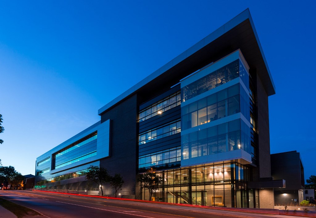
University of Ottawa
Advanced Research Complex (ARC)
25 Templeton Street
Room ARC 233
Previous seminars
| Date | Presenter | Title | Abstract | Links |
|---|---|---|---|---|
| January 25th, 2024 | Assistant Professor Sergio de la Barrera, Department of Physics, University of Toronto | Emergent symmetries and properties in graphene multilayers | Graphene is a beautiful and incredibly versatile platform for investigating emergent electronic phenomena. Confining electrons to two dimensions enhances their influence on one another, and empowers us to alter their environment with external fields and additional layers. Strategic combinations and arrangements of layered materials can yield new physics and surprising electronic properties. This seminar presents how certain combinations lead to superconductivity, magnetism, and topology from materials that have none of these properties on their own, and how they can address essential questions in quantum materials research. | Read more |
| February 29th, 2024 February29th2024 | Postdoctoral Fellow Bowen Yang, Institute for Quantum Computing, University of Waterloo | Probing 2D and Moiré Magnetism through Tunneling Transport | A series of results is presented on a two-dimensional (2D) magnetic material, CrI3, in the atomically thin limit and in a twisted structure, using electrical tunneling transport and/or spectroscopy. In the former, the research group discovers over one million percent of magnetoresistance and obtain a simple microscopic Hamiltonian describing the 2D spin system. In the latter, they find new hysteretic and anisotropic field evolution of the magnetization behavior, arising from coexistence of AFM and FM interlayer interactions. They further uncover two distinct non-volatile spin textures at around 1 degree twist angle with different tunneling resistance that can be switched by magnetic field. | Video link iewseminar |
March 21st, 2024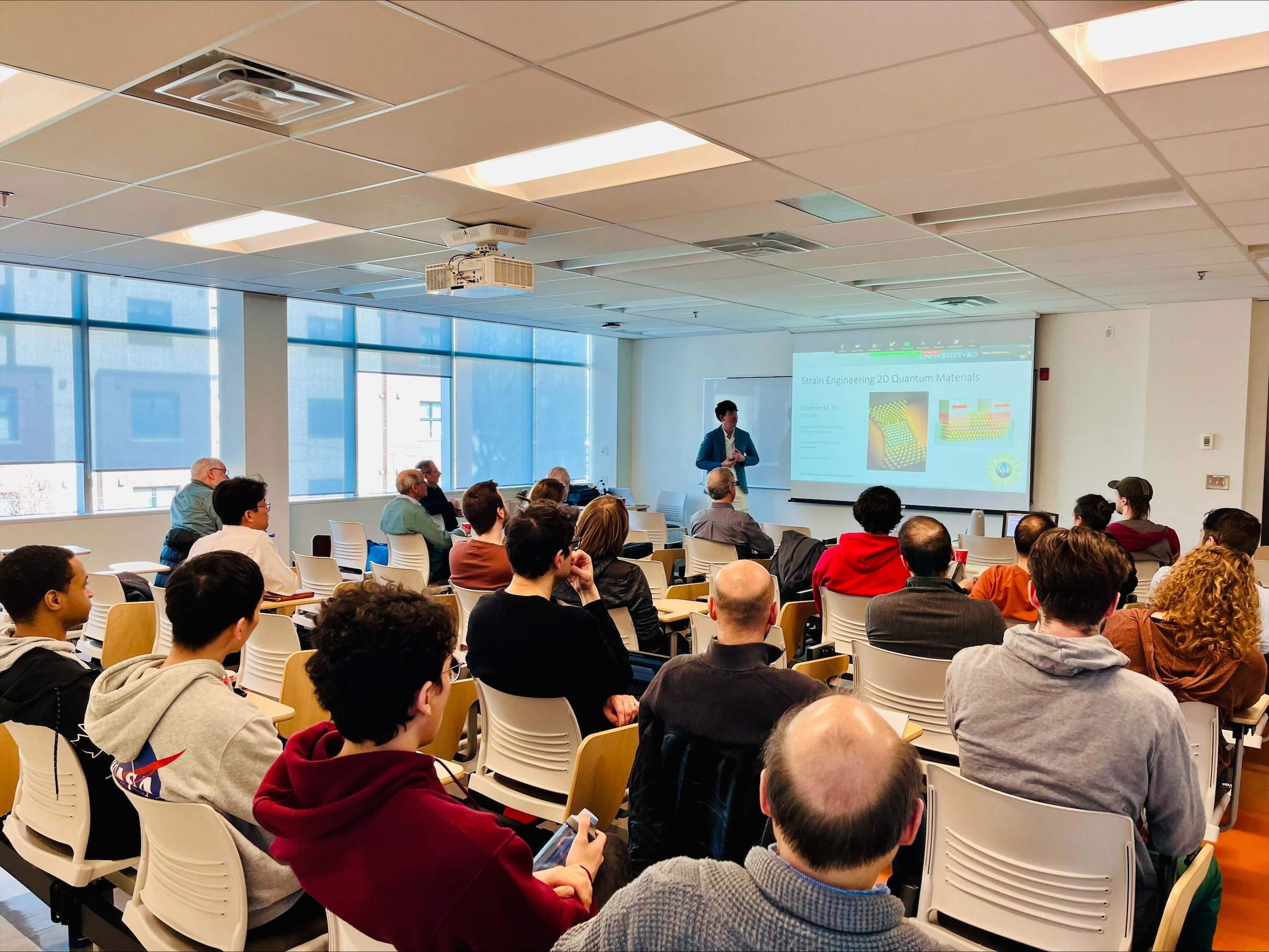 | Assistant Professor Stephen M. Wu, Department of Electrical and Computer Engineering, University of Rochester | Strain engineering 2D quantum materials | Strain engineering in electronics has been widely utilized over the last 20 years to enhance carrier mobility in most standard Si-based CMOS fabrication processes. These process-induced strain engineering techniques, engineered from the nanofabrication process itself, are simple, reliable, applied device-to-device, and highly scalable down to the nanometer scale. In this talk, Prof. Stephen M. Wu introduces his group work in exploring how process-induced strain engineering translates to the world of 2D materials, and how this may be applied to engineer quantum materials properties. Control over the strain degree-of-freedom in 2D materials opens new pathways for exploration in engineered quantum materials, since strain in weakly-bonded 2D systems can go far beyond strain-engineering in conventional 3D-bonded materials. This is discussed in the context of two different ongoing projects in Prof. Wu group: 2D straintronic phase-change transistors/memristors, and moiré superlattice engineering with strain in twisted and untwisted bilayer 2D heterostructures. | Read more Video link |
| May 13th, 2024 | PhD Student Alina Wania Rodrigues, Quantum Theory Group, University of Ottawa | Designing programmable simulators of strongly correlated electron systems in 2D materials | In this work, we present a Hofstadter’s butterfly spectrum for the magic angle twisted bilayer graphene (MATBG) obtained using an abinitio based multi-million atom tight-binding model. We incorporate a hexagonal boron nitride substrate and out-of-plane atomic relaxation. The effects of a magnetic field are introduced via the Peierls modification of the long-range tight-binding matrix elements and the Zeeman spin splitting effects. A nanoribbon geometry is studied, and the quantum size effects for the sample widths up to 1μ are analyzed both for a large energy window and for the flatband around the Fermi level. For sufficiently wide ribbons, where the role of the finite geometry is minimized, we obtain and plot the Hofstadter spectrum and identify the in-gap Chern numbers by counting the total number of chiral edge states crossing these gaps. Subsequently, we examine the Wannier diagrams to identify the insulating states at charge neutrality. | Read more Video link |
| June 27th, 2024 | Postdoctoral Fellow Ayse Melis Aygar, Electrical Engineering, McGill University | High-Density, Flip-Chip Alkali Doping of Graphene and Observation of the Lifshitz Transition | Experimental setups for charge transport measurements are typically not compatible with the ultrahigh vacuum conditions for chemical doping, limiting the charge carrier density that can be investigated by transport methods. Field-effect methods, including dielectric gating and ionic liquid gating, achieve too low a carrier density to induce electronic phase transitions. To bridge this gap, we developed an integrated flip-chip method to dope graphene by alkali vapor in the diffusive regime, suitable for charge transport measurements at ultrahigh charge carrier density. We introduce a cesium droplet into a sealed cavity filled with inert gas to dope a monolayer graphene sample by the process of cesium atom diffusion, adsorption, and ionization at the graphene surface, with doping beyond an electron density of 4.7 × 1014 cm−2 monitored by operando Hall measurement. The sealed assembly is stable against oxidation, enabling measurement of charge transport versus temperature and magnetic field. Cyclotron mass inversion is observed via the Hall effect, indicative of the change in Fermi surface geometry associated with the Liftshitz transition at the hyperbolic M point of monolayer graphene. The transparent quartz substrate also functions as an optical window, enabling nonresonant Raman scattering. Our findings show that chemical doping, hitherto restricted to ultrahigh vacuum, can be applied in a diffusive regime at ambient pressure in an inert gas environment and thus enable charge transport studies in standard cryogenic environments. | Read more Video link |
| October 3rd, 2024 | Dr. Marek Potemski, LNCMI-Grenoble, CNRS France | Magnons, magnon polarons and spin-entangled optical resonances in semiconducting van der Waals antiferromagnet | Two-dimensional materials beyond graphene offer a remarkable platform for exploring the unique electronic, optical, and magnetic properties of low-dimensional systems. Among these are van der Waals layered magnets, particularly the family of metal phosphorus trichalcogenides (MPX3, where M = Mn, Fe, Co, Ni, and X = S, Se). These MPX3 compounds are semiconducting antiferromagnets with varied spin-ordering configurations. This talk will present the results of magneto-spectroscopy studies (Raman scattering, far- and near-infrared optics, EPR) on several representative layered antiferromagnets, including MnPS3, MnPSe3, FePS3, FePSe3, NiPS3, and CoPS3. The focus will be on identifying the diverse spectra of magnon-gap excitations, exploring magnon-phonon coupling, and discussing the origin of the intriguing spin-entangled optical transitions observed in certain materials in this class. | Read more Video link |
| December 5th, 2024 | Dr. Ziliang Ye, University of British Columbia | Sliding ferroelectricity in rhombohedral MoS2: from slip avalanche to non-volatile optical memory | The tunability in the stacking degree of freedom of van der Waals materials provides a new and powerful approach to engineer their physical properties. Sliding ferroelectricity is one such example that has been observed in artificially stacked boron nitrides and transition metal dichalcogenides, where an electric field can drive one layer of materials to move relative to its neighbors due to an out-of-plane electric polarization arising from coupling between adjacent layers. In this talk, I will show that such a hysteretic phenomenon can also occur in chemically synthesized rhombohedral molybdenum disulfide (3R-MoS2). Due to an unavoidable shear force during crystal exfoliation, avalanches of interlayer slips can happen, resulting in a variety of differently stacked domains with a power-law size distribution. When the external electric field overcomes the local pinning, these pre-existing domain walls can be released for propagation, switching the polarization over a large area of the flake. Thanks to the strong excitonic effects in 3R-MoS2, such atomic-scale motion can be resolved using visible light. The stacking switch induces a large reflectance contrast on an ultrafast timescale, allowing it to be built into non-volatile optical memories with high performances. | Video link |
January 16th, 2025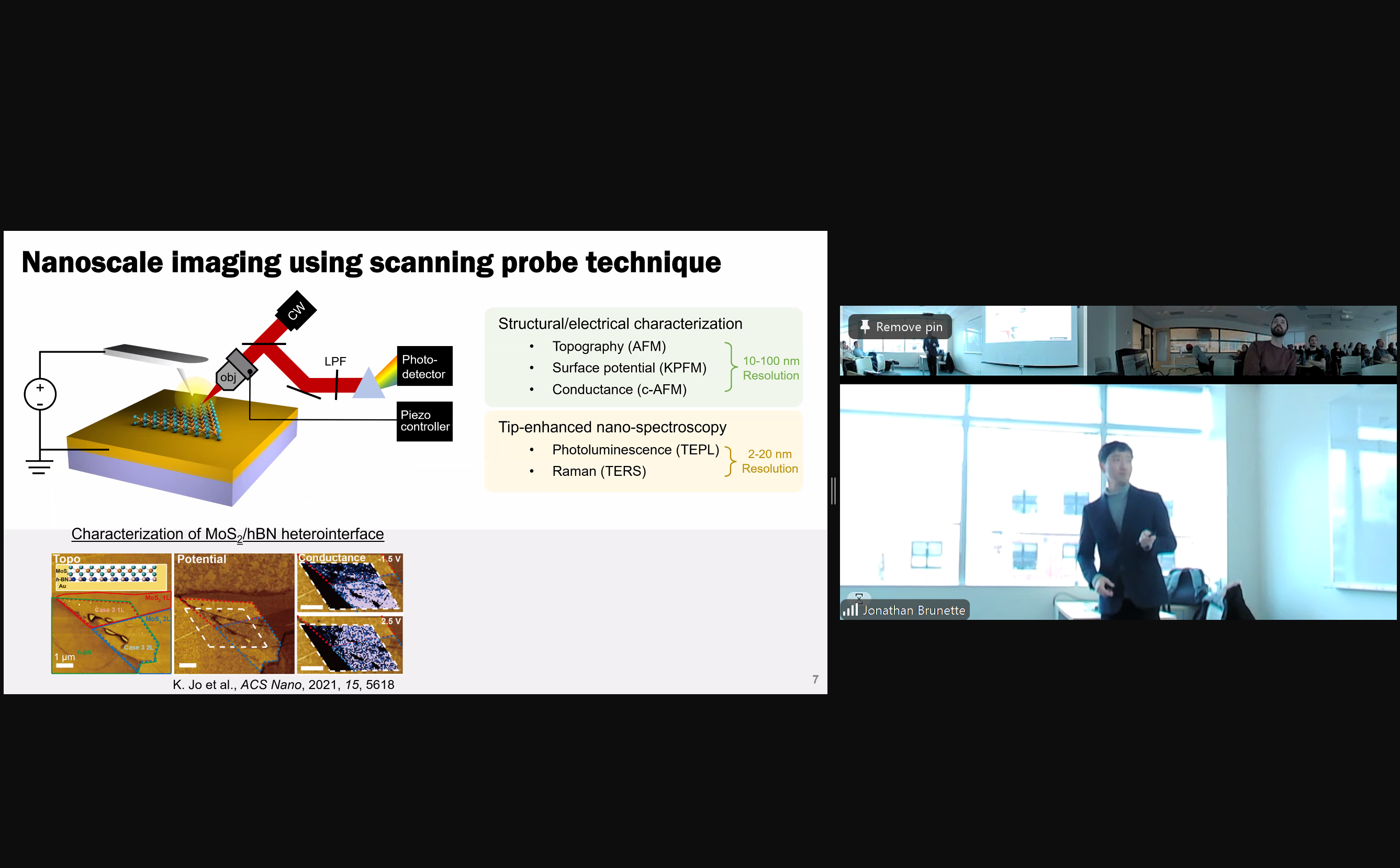 | Dr. Kiyoung Jo, University of Pennsylvania | Direct sub-wavelength imaging of optoelectronic properties at 2-dimensional semiconductor- metal interfaces | Metal contact to two-dimensional semiconductors is one of the most consequential aspects for achieving high-performance and large-scale electronic and optoelectronic devices. As semiconductor materials are thinned down to the nanometer limit, the contact becomes a dominant factor governing device behavior. However, the chemistry of the contact remains poorly understood because semiconductor-metal contacts are buried interfaces, making them difficult to probe directly. In the first part of this talk, I will present spatial imaging of optoelectronic characteristics of 2D transition metal dichalcogenides (TMD)- metal interfaces. Using a unique metal assisted flipping technique, we are able to access TMD contacts with various metals (Au, Ag and In) to probe their electrical and optical properties. By leveraging scanning probe microscopy coupled with spectroscopy, we performed kelvin probe force microscopy, conductive-AFM, tip-enhanced Raman and photoluminescence spectroscopy. This approach enables concurrent mapping of electrical potential, conductivity, strain and emission spectra at the interface with deep-subwavelength (5-20 nm) spatial resolution. In the second part, we will discuss the excitonic emission within strain-localized WSe2 nanobubbles (50-100 nm in diameters) under different electrical contact environments, such as Schottky and Ohmic contacts. We found the types of the surrounding contact significantly influences the excitonic emission of these nano-emitters, enabling changing the excitonic emission via electrical polarity. At Schottky interfaces, core/shell-like emissions are observed within the nanobubbles, whereas Ohmic contacts exhibit only strain-localized excitons. The strategies presented in this talk will provide insights for investigating diverse nanomaterial systems for applications in nano-electronics and photonics. | |
| May 22nd, 2025 | Dr. Louis Gaudreau, University of Ottawa & NRC | A new platform for quantum electronics based on 2D semiconductors | Monolayer transition metal dichalcogenides have emerged as prominent candidates to explore the complex interplay between the spin and the valleys degrees of freedom. The strong spin-orbit interaction and broken inversion symmetry within these materials lead to the spin-valley locking effect, in which carriers occupying the K and K’ valleys of the reciprocal space must have opposite spin depending on which valley they reside. This effect is particularly strong for holes due to a larger spin-orbit gap in the valence band. By reducing the dimensionality of a monolayer of tungsten diselenide to 1D via electrostatic confinement, we demonstrate that spin-valley locking in combination with strong hole-hole interactions lead to a ferromagnetic state in which hole transport through the 1D system is spin-valley polarized, even without an applied magnetic field, and that the persistence of this spin-valley polarized configuration can be tuned by a global back-gate. This observation opens the possibility of implementing a robust and stable valley polarized system, essential for valleytronic applications. | Video link |
| Sept 18th, 2025 | Dr. Giulio Vampa, NRC, JASLab & JCEP | Interacting intense laser fields with quantum light and quantum materials | Quantum light, typically having few photons, and attosecond science, which utilizes intense laser fields, have seemingly nothing in common. In my talk I will challenge this preconception. We perturb the emission of high-order harmonics from a semiconductor with a quantum-optical state, bright squeezed vacuum, to generate sidebands of the high harmonics that exhibit super-Poissonian (i.e. bunched)photon statistics. Our results suggest that perturbing strong-field dynamics with quantum-optical states is a viable way to coherently control the generation of such states at short wavelengths, possibly even in the extreme ultraviolet or soft X-rays. Our theoretical analysis indicates that the technique entangles the high-order sidebands with the squeezed vacuum perturbation, paving the way for the creation of non-Gaussian states with projective measurements. In addition, I will show how we utilize an attosecond field-sampling technique, to sample the field of a squeezed vacuum beam. We reveal the temporal modal structure of femtosecond bright squeezed vacuum, as well as the random flips of the sign of the carrier wave and exploit them to crate a quantum random number generator, with potentially PHz bandwidth. Quantum correlations will be instrumental to advance attosecond spectroscopy and imaging beyond the classical limits. If time permits, I will also present our latest results in establishing high-harmonic spectroscopy of phonon dynamics in WTe2. | |
| Jan 22nd, 2025 | Dr. Vedran Jelic, NRC | Ultrafast Lightwave Microscopy and Spectroscopy of Quantum Materials with Atomic Resolution | Ultrafast control and characterization of electronic and structural dynamics are key to understanding emergent phases in quantum materials. In this talk, I will present two complementary lightwave-driven approaches for microscopy and spectroscopy that I have led the development of, and illustrate their capabilities through studies of the type-II Weyl semimetal WTe2 as a model system for nonequilibrium dynamics. Lightwave-driven terahertz scanning tunneling microscopy (THz-STM) combines single-cycle terahertz pulses with STM to simultaneously achieve picometer spatial resolution and femtosecond temporal resolution, thereby overcoming a longstanding disconnect between ultrafast spectroscopy and atomic-scale imaging of surfaces. In parallel, time-resolved high harmonic spectroscopy (tr-HHS) is established as an all-optical probe of coherent lattice motion, with phonon-driven modulations of the electronic band structure encoded in the high harmonic emission, providing femtosecond-resolved access to momentum space dynamics. Together, these two newly developed techniques enable a unified view of ultrafast phenomena in quantum materials by linking atomic-scale real-space dynamics to the ultrafast evolution of the electronic band structure with unprecedented precision. While demonstrated here for layered van der Waals WTe2, the approach is broadly applicable to other systems, including two-dimensional materials, opening new opportunities for studying ultrafast electron–phonon coupling, sub-cycle control of band topology, and the emergence of nonequilibrium phases. |